Emerging thin film photovoltaic technologies, currently being developed in research laboratories, are the EU’s key to unlocking its photovoltaic industry and ensuring the growth of a sustainable and green electricity market
The European Green Deal and its Fit for 55 initiative aim to transform Europe into a modern, resource-efficient and competitive economy, ensuring the reduction of net greenhouse gas emissions by at least 55% by 2030, compared to 1990 levels.
Solar photovoltaics is considered as one of the cornerstones to achieve a green and carbon-neutral future. As the lowest-cost and most easily deployed clean energy technology, the installed photovoltaic (PV) capacity in Europe has reached almost 195 GW in 2022, and the REPowerEU plan targets to bring online over 320 GW of solar photovoltaic by 2025 and almost 600 GW by 2030.
Today, most photovoltaic panels and/or their constitutes are imported to the European Union (EU). China accounts for around 75% of the global PV module and 97% of the wafer production. According to the SolarPower Europe’s PV manufacturing map, there is around 70 GW p/a of Si technologies production along the value chain, including module, solar cells, ingot and wafer, poly-Si and mg-Si, in Europe. There is currently no thin film production above pilot level in Europe.
To reach the EU targets towards a carbon-neutral continent, ensure the growth of sustainable and green electricity market, and to reduce dependence on imports of PV technology, it is essential to increase the competitiveness of EU’s PV industry and offer a variety of innovative PV products that meet the high standards of EU consumers.
Thin film PV technologies are what the EU photovoltaics industry needs
Thin film PV technologies can play an important role in developing a robust PV industry in Europe, as they hold the promise for providing cheap, resource saving and scalable technologies for the PV market as well as new and versatile applications such as tandem, transparent, flexible building and product integrated photovoltaics.
Thin film technologies such as CIGSe and CdTe are on the market, however there is no production above pilot level in Europe. Several emerging thin film PV technologies such as perovskite, organics, CZTS have been under development for more than a decade and reach the efficiencies of 26.1, 19.2 and 14.9 %, respectively. (1)
A complementing materials system is the Sb-chalcogenide (Sb2Se3, Sb2S3 and Sb2(S,Se)3), which, while being relatively unexplored, have reached efficiency of 10.7%. (2) Today, it is still unclear which emerging thin film technologies will make the market, thus extensive further R&D in all the above-mentioned materials is essential.
What we do in the frame of 5GSOLAR project
The 5GSOLAR project provides the coordination and support action frame on the development of emerging inorganic earth-abundant thin film chalcogenide materials. Our specific attention is on development of antimony and bismuth-based chalcogenides Sb2(S,Se)3, (Sb,Bi)2Se3 and their alloys. These materials are in the scientific spotlight due to several noticeable features such as tuneable bandgap (1.0-1.8 eV), high absorption coefficient (>105 cm-1), long-term stability, and earth-abundant constituents.
Moreover, they can be processed at relatively low temperatures (below 300°C) by applying technologies in use in classical thin film PV technology (e.g., CdTe and CIGS). Such material properties offer a broad range of device concepts for various applications – from classical thin film approaches towards semi-transparent and breaking-up forward to tandem/multi-junction architectures, thus allowing a wider application range than traditional Si-based modules, including also but not limited to building and product integrated PV.
We focus on materials development using rapid deposition approaches, combining robust, resource-saving, high yield and easily scalable ultrasonic chemical spray pyrolysis and close spaced sublimation techniques.
Close spaced sublimation is the simplest, fastest, and most resource-saving technology among physical thin film deposition methods and is the dominant method in use for commercial CdTe thin film SC. Feasibility of this processing technique has been proven for Sb2Se3 in laboratory scale, reaching the efficiency of about 8%. (3, 4)
Chemical spray pyrolysis has the potential to become the frontline technology for fabrication of thin film solar cells. The Sb2Se3 solar cells under the development in the lab, both electron transport layer and absorber layer are deposited by chemical spray pyrolysis method. The unique feature is that the device is fabricated in ambient atmosphere, and there is no need of the glove box in any stage of the thin film deposition. On top of that, the chemical spray pyrolysis is extremely resource-saving technology. For example, 1 kg of antimony is enough to cover 5,000m2 of a substrate with a 100 nm thick Sb2S3 layer by spray. Thus, remarkable PV fabrication cost and materials reduction can be foreseen.
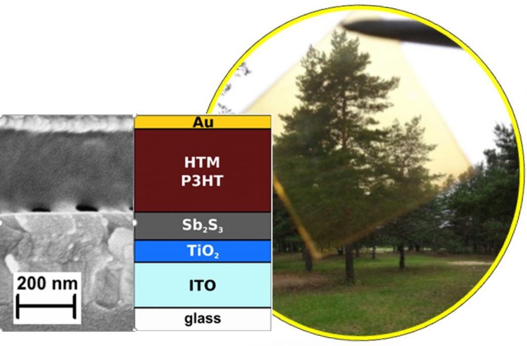
In the present stage of solar cell development, a solar cell stack comprising of glass/conductive oxide/TiO2 (thickness around 30 nm) /Sb2S3 (thickness around 80 nm)/hole conductor/metal contact results in a power conversion efficiency of 6.0% and average visible transparency of around 35%.
The main stack of the solar cell is fabricated in less than 1.5 h by chemical spray pyrolysis method and practically adds no extra weight (<10 g/m2) to the substrate. The preliminary results show that the Sb2S3 thin film solar cell fabricated by chemical spray pyrolysis has the potential to be applied in semi-transparent application. (5)


This work is licensed under Creative Commons Attribution-NonCommercial-NoDerivatives 4.0 International.


