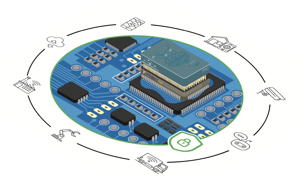
Dr. Fabio Pavanello, Researcher at CNRS/CROMA Laboratory, guides us through a novel route to secure and low-power accelerators for edge computing, or in other words, the NEUROPULS approach
The current exponential increase of devices at the edge demands ever-growing performance to process vast amounts of locally generated data daily.
Specialised hardware solutions are under investigation to achieve ultra-low-power computation while being lightweight, cost-effective, and commercially scalable. Additionally, such solutions shall also be highly secure, e.g., for data integrity and confidentiality, and, depending on the application, should provide extremely low latencies, e.g., in safety-critical scenarios (autonomous driving, healthcare, aviation, etc.).
Among the different approaches currently pursued, neuromorphic computing has gathered significant attention because of its potential to process data more efficiently by drawing inspiration directly from how the human brain works.
The role of integrated photonics in the computing race
Among the different technologies considered to build neuromorphic systems, integrated photonics has appeared as a potential candidate for next-generation computing systems. Several advantages compared to competing technologies, e.g., electronics or spintronics, come directly from the physical nature of light and how it propagates.
By using integrated approaches, light signals carrying large bandwidth data can be propagated in tiny sub-μm optical waveguides, while being manipulated along their path with ultra-low optical losses.
Data encoding onto the several degrees of freedom available for light signals, such as frequency, amplitude, phase, and polarisation, allows photonic systems to achieve a large throughput (compute density), despite the larger dimensions of photonic circuits compared to their electronic counterparts.
Advances in integrated photonics allow the manipulation of light signals at speeds far exceeding those achievable in electronics. For example, data encoding and retrieval at hundreds of Gbit/s onto a single frequency channel can be achieved by using high-speed (>50 GHz) optical modulators and detectors in silicon photonic platforms, as well as high-bit density modulation formats and coherent approaches. However, current CMOS-compatible silicon photonic platforms have been developed with the initial goal of building high-speed optical interconnects rather than computing systems.
Therefore, one of the major challenges currently faced is achieving ultra-low-power neuromorphic photonic systems while employing CMOS-compatible platforms for volume scalability. This challenge requires advances at the material, device, and system levels to address the need for such computing systems to be deployed at the edge.
Augmented silicon photonics platforms
Current silicon photonic platforms, leveraged for applications ranging from communications to sensing, lack two key ingredients that, integrated within the same platform, would be highly beneficial for neuromorphic photonic systems.
On the one hand, integrated III-V sources allow for better system compactness, a reduced number of optical interfaces (with their associated losses), and the capability of building high-speed spiking neurons, thus removing the need for optical signal amplification in multi-layer architectures.
On the other hand, phase-change materials (PCMs) integrated onto silicon waveguides allow for non-volatile reconfigurability, which is essential for holding a specific neural network configuration in a lossless manner, i.e., where energy is not dissipated to hold a given set of weights during the inference phase. Besides, their fast dynamics and non-volatile reconfigurability by means of ultra-short optical or electrical pulses open the doors for on-chip training by leveraging emergent plasticity approaches.
In the Horizon Europe Research and Innovation Action (RIA) project NEUROPULS (NEUROmorphic energy-efficient secure accelerators based on Phase change materials aUgmented siLicon photonicS), we are introducing both III-V materials as well as PCMs in an existing 300-mm-wafer silicon photonic platform developed at CEA-LETI (France).
The introduction of these materials and the resulting novel photonic devices and architectures will enable us to achieve an ultra-low-power (well below 1 pJ/MAC) neuromorphic accelerator implemented on a single photonic integrated circuit (PIC) chip for edge computing. More specifically, its performance will be proven in three industry-relevant use cases jointly with the industrial partners involved in the project.
Cybersecurity challenges and the need for novel technologies
To deploy computing systems at the edge, strong security layers are present to guarantee a series of services that are essential in data processing, such as data confidentiality and integrity or accelerator authentication towards an edge node or server. While common strategies use cryptographic protocols combined with data stored in non-volatile memory (e.g., secret key in AES protocol), the potential of accessing memory sectors by leveraging hardware and software vulnerabilities calls for novel technologies.
Among the different solutions that are currently investigated, hardware primitives like physical unclonable functions (PUFs) are regarded as viable solutions to counteract memory-prone security attacks. PUFs permit the real-time generation of keys without the need for permanent key storage. However, current electronic-based PUF solutions present a series of drawbacks that are still posing a significant challenge to their large-scale deployment in edge systems.
In NEUROPULS, we are investigating how to build photonic PUFs leveraging the benefits provided by our augmented silicon photonics platform to achieve a superior strength to, e.g., modeling or side-channel attacks compared to electronic-based solutions such as arbiter PUFs.
High-level simulation of complex RISC-V-interfaced SoCs Co-design of photonic accelerators with electronic processors is fundamental to achieving optimal performance at a full system level. However, no open-access simulation platforms currently exist to address this challenge.
One of NEUROPULS’s main contributions is the development of a unified simulation framework based on GEM5.
This framework will allow us to model the behaviour of the photonic accelerator and its security layers once interfaced with an open-source RISC-V processor embedded in an electronic integrated circuit (EIC) next to the accelerator’s drivers. Such a framework will be vital in exploring different scenarios to optimise our computing electronic-photonic platform, extract relevant metrics, and predict performance beyond what will be explored in our prototype.

This work is licensed under Creative Commons Attribution-NonCommercial-NoDerivatives 4.0 International.


