Thomas W. Hansen, Senior Scientist at DTU Nanolab, Technical University of Denmark details an aspect of materials science that concerns the role of nanostructures and nanoparticles in contemporary society. Much of the discussion focuses on why a fundamental property of these materials is the melting point
Nanostructures in general and nanoparticles, in particular, play an increasing role in contemporary society – especially in catalysis where materials often consist of metal nanoparticles – supported on a substrate, this class of materials play a pivotal role.
Catalytic reactions occur at surfaces where reactants can absorb, dissociate and combine into products of higher value. The metallic nanoparticulate component of the catalyst is often a precious metal, for example, platinum group metals (palladium, platinum, ruthenium…), hence it is important to get as much surface area from as small a volume as possible. However, as the defining size of such structures decreases into the sub-10 nm regime, their properties start to diverge from their bulk counterparts.

When trying to extract specific size dependent fundamental properties from a sample, it is highly beneficial to have a large ensemble of particles with narrow size distribution. Such samples are challenging to prepare by taking the chemical route. However, a cluster source with a mass separation system allows for samples with narrow size distributions (below 0.5 nm).1 Extracted parameters will then no longer rely on continuously keeping the same nanoparticle in the field of view and statistics are extracted more easily.
The melting point
One such fundamental property is the melting point. The depression of the melting point was investigated in depth by Buffat and Borel in 1976 using diffraction techniques on ensembles of nanoparticles.2 Recently we investigated the melting temperature of both ensembles with narrow size distributions as well as individual gold nanoparticles using high-resolution transmission electron microscopy in combination with molecular dynamics calculations (MD).3 The local information provided by microscopy sheds light on not only the melting point but also the melting process itself.
Gold nanoparticles with diameters around 5 nm, 3 nm and 1.9 nm (designated as Experiment 1, 2 and 3 respectively) produced with a cluster source was deposited on a MEMS fabricated heating chip with a silicon nitride membrane from DENSsolutions. These chips allow imaging at the deep sub-nm scale while increasing the temperature up to 1300°C. For imaging, an aberration-corrected FEI Titan 80-300 transmission electron microscope was used, the microscope is equipped with a OneView camera from Gatan which provides a good combination of speed and sensitivity. In order to image the melting process, the samples were first heated to temperatures a few tens of degrees below the expected melting point in a single step. After observing a stable crystalline sample exposing lattice fringes in the TEM image, the temperature was gradually increased until the lattice fringes were no longer observed (interpreted as molten) at which point the exact particle diameter and temperature was logged.

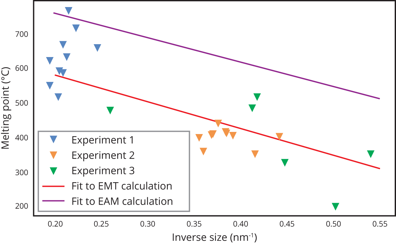
The results showed a significant drop in melting point (Figure 1), decreasing with size despite a significant scatter in the results, particularly for the largest particles. As the temperature approaches the melting point, the particles become increasingly mobile. For the MD calculations, both Effective Medium Theory, as well as the Embedded Atom Model, were used for the interatomic potentials. Figure 1 shows the comparison between the experimentally observed melting points as well as the MD results using both approaches.
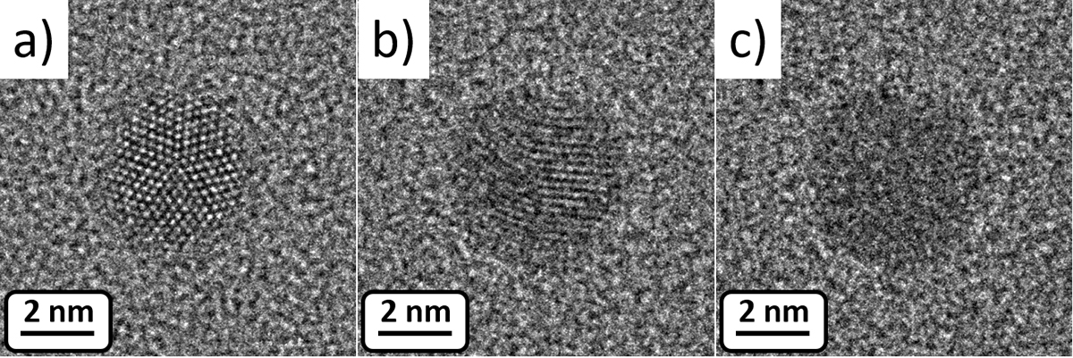
However, for applications where surface properties are important, for example, catalysis, the exact melting process is of higher importance than the state of the interior of the particle. This is the type of information that can be derived from high-resolution transmission electron micrographs. Figure 2 shows three frames from an image sequence acquire at 612°C. In frame a), the crystalline lattice is clearly resolved with the five-fold symmetry, which is typically observed for gold nanoparticles. The crystalline particle is surrounded by a halo, which we interpret as mobile atoms (i.e. molten). Frame b) still shows fringes but not as clear. In frame c) which is acquired 0.2 seconds after frame b), no fringes are observed and the particle is molten.
Conclusion
Our experiments indicate that a pre-molten surface exits prior to complete melting. Such a mobile surface should be taken into account when investigating phenomena occurring at elevated temperatures. The results indicate how technological advancements such as MEMS heaters and aberration correctors can provide new insight into materials science.
References
1 P. Hernandez-Fernandez, F. Masini, D. N. McCarthy, C. E. Strebel, D. Friebel, D. Deiana, P. Malacrida, A. Nierhoff, A. Bodin, A. M. Wise, J. H. Nielsen, T. W. Hansen, A. Nilsson, I. E. L. Stephens, and I. Chorkendorff, Nat. Chem. 2014, 6, 732.
2 P. Buffat and J.-P. Borel, Phys. Rev. A 1976, 13, 2287.
3 P. Schlexer, A. B. Andersen, B. Sebok, I. Chorkendorff, J. Schiøtz, and T. W. Hansen, Part. Part. Syst. Charact. 2019.
Please note: This is a commercial profile
Thomas W. Hansen
Senior Scientist
DTU Nanolab, Technical University of Denmark
Tel: +45 4525 6476


